

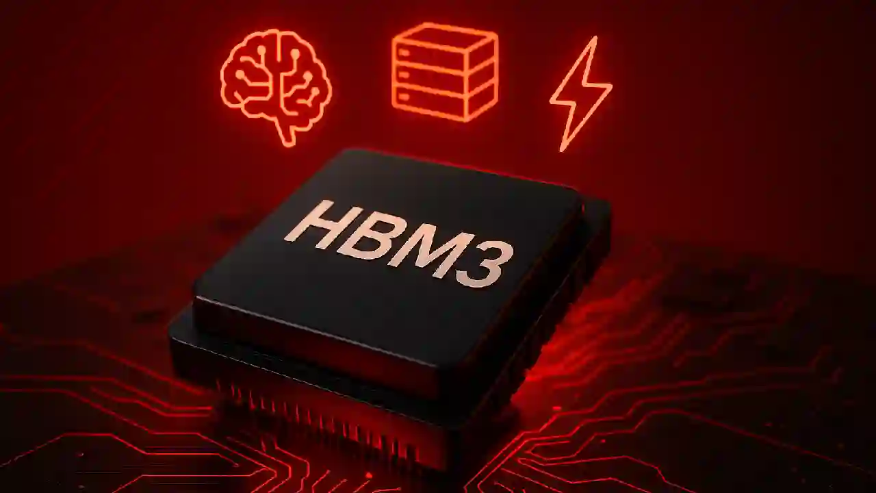
The 3D-stacked DRAM interface known as High-speed Memory 3 (HBM3) can handle up to 819 GB/s of speed per stack. It has a 1024-bit bus and a silicon interposer that let it offer high throughput with low power. This makes it perfect for AI, HPC, and tasks that need to process a lot of data.
Simple memory can’t keep up with training huge AI models like GPT or running the fastest computers in the world. That’s where HBM3, or High Bandwidth Memory 3, comes in. It’s a huge step forward in memory technology that puts speed, small size, and power economy first.
This blog post will explain HBM3 in simple terms, talk about why it’s important for AI and HPC, and take a look at what HBM3E and HBM4 have in store for the future.
What is HBM3 and why it matters
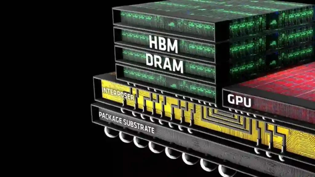
High Bandwidth Memory 3 (HBM3) is the third version of this next-generation memory interface made for very fast computing. Instead of using flat chips like DDR5 or GDDR6, HBM3 stacks memory vertically using a 3D architecture. It is linked with ultra-wide channels to provide a huge bandwidth in a very small space.


As you might know, this is a big deal when you’re using a supercomputer to run exercises or train big language models like Llama 3. With HBM3, you can do that faster and with less power than ever before.
How HBM3 works in simple words
Imagine putting several pancakes (memory dies) on top of each other and running syrup (data) through tiny straws (TSVs) that are placed between them. Now put the stack next to the CPU and GPU and use a special tray (silicon interposer) to connect them. That’s how HBM3 is put together.
Here’s what makes it work:
- 3D-stacked DRAM: Memory layers are stacked vertically to save space
- 1024-bit wide interface: Much wider than DDR5’s 64-bit channels
- Through-Silicon Vias (TSVs): Micro-connections that let data flow vertically
- 2.5D packaging with silicon interposer: Ensures high-speed connection between processor and memory
All this enables lightning-fast data movement with minimal power loss.
Key features and real-life benefits
Here’s why HBM3 stands out:
Bandwidth Beast
- 819 GB/s per stack — nearly 4x faster than GDDR6
- Some vendors like Rambus even push over 1 TB/s per device
Power Efficient by Design
- Lower operating voltage (1.1V vs HBM2E’s 1.2V)
- Efficient signaling with just 400mV IO levels
- Reduces heat, ideal for power-hungry data centers
More Memory in Less Space
- Up to 24 GB per stack using 12-high die stacks
- Multiple stacks = 96 GB+ of near-processor memory
Built-in Reliability
- Advanced ECC, adaptive refresh, and thermal-aware management
- Reduces data errors during high-speed processing
Pros and cons of HBM3
| Aspect | HBM3 Advantage | Trade-off |
|---|---|---|
| Speed | Unmatched bandwidth per watt | More complex interconnect design |
| Power Efficiency | Lower voltage, reduced heat | Needs better cooling for dense stacks |
| Space Optimization | Compact 3D stacking | Challenging to manufacture at high yields |
| Reliability | ECC, refresh control, lower error rates | Expensive compared to traditional memory |
What comes after HBM3?
HBM3E – Going beyond the standard
- Data rates up to 9.8 Gb/s per pin
- 1+ TB/s throughput per stack
- Already shipping with NVIDIA’s Blackwell GPUs
HBM4 – The future of memory
- 2048-bit wide interfaces
- Up to 64 GB per stack
- Bandwidth per device to exceed 1.6 TB/s
- Launch expected by 2026
R&D Frontiers
- Optical interconnects for lower power
- Cryogenic memory for quantum computing
- Integration into chiplet-based systems for edge AI
Conclusion
HBM3 is more than just another memory spec — it’s a critical enabler of the AI revolution. With its high bandwidth, compact size, and power-saving design, it fuels everything from GPT-scale models to real-time edge AI. As we move into the era of HBM3E and HBM4, this memory tech is shaping the backbone of next-gen computing.
Would you explore HBM3-powered systems for your AI workloads? Let us know.